
Breaking Beautiful
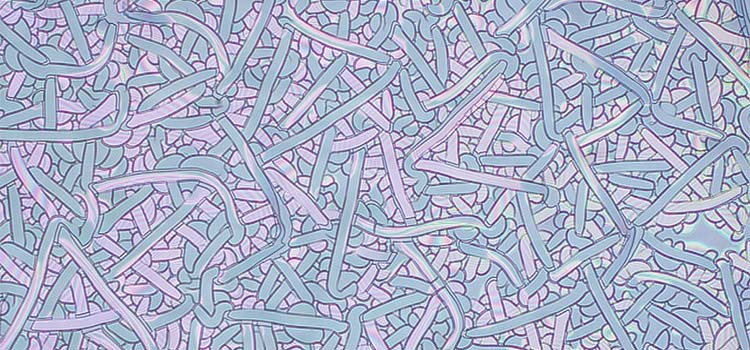
High resolution photograph of cracks in thin layer of glass atop a silicon wafer. The colors come from optical interference between the thin wafer and the glass above.
Joël Marthelot (ESPCI)
Image rights: Used with permission.
(Inside Science) -- Repeating crescents, snail shell-like spirals and a jumble of shapes resembling a Keith Haring painting: These patterns and more can start to adorn old paintings, pottery glazes and even electronics under the right conditions. Now, a team of scientists from France and Chile has revealed the potentially useful mechanism that causes these beautiful but often damaging cracks.
“I think it’s very creative work,” said John Hutchinson, a mechanical engineer at Harvard University in Cambridge, Massachusetts. “These crack patterns are extraordinary.”
The research team first learned about crescent-shaped cracks from a physicist at the Ecole Normale Supérieure de Cachan in France; she noticed the cracks forming on tiny optical devices she had designed. The team then discovered other examples of unusual, highly ordered cracks in previously published papers by different research groups. Some of these patterns had apparently gone unnoticed even by the authors of those studies.
Nobody seemed to know why such cracks occur. Cracks that appear on thin films like paint, mud and pottery glazes typically grow randomly, with new fractures shooting off at right angles from existing ones. The scientists realized they were seeing a completely different type of crack that grows nonrandomly and can make intricate, orderly patterns in surfaces.
To better understand how the cracks form and grow, the research team deposited spin-on glass, a material commonly used in electronics, onto silicon wafers. The scientists then varied parameters like the glass' thickness and the strength of the adhesion between the glass and the silicon. Under the right conditions, cracks started forming from impurities in the glass or from scratches that the researchers made in the film, and created spirals, crescents and other repeating patterns.
The researchers discovered that for the patterned cracking to occur, the glass had to both fracture and separate from the silicon. As a result, cracks only appeared when the thin film of glass did not adhere strongly to the silicon wafer beneath it. Additionally, if the film was too tough, or resistant to fracturing, cracks did not form.
The scientists also found that regardless of the specific pattern formed, the width of the repeating pattern created by the cracks was always around 32 times the film’s thickness. Similar results have appeared in previous studies, said study coauthor Benoît Roman of the École Supérieure de Physique et de Chimie Industrielles in Paris. The width-to-thickness ratio “is very robust,” he said. “You can see it in many different materials.”
By systematically altering the chemical and physical properties of their glass film, the researchers mapped out the conditions under which the spiral- and crescent-shaped cracks grow. The specific pattern formed depends on the exact shape of the defect that initiates the crack.
In 2012, a research team in Korea controllably grew orderly cracks in a thin film, although that team used a different film material and created a limited variety of shapes.
Because the cracks his team studied rely on a film adhering weakly to a surface, Roman said they are unlikely to appear in conventional commercial products, where films are usually strongly bonded to surfaces. So his team’s findings are unlikely to help design anti-reflective or non-stick coatings, which can crack due to other processes.
“In most cases people make an effort to have very good adhesion with the substrate,” he said.
The team’s findings could, however, help reduce cracking in newer applications involving coatings on soft materials, such as stretchable electronics, organic LED sheets or fuel cells. In these situations adhesion between film and underlying structure is often weaker.
Orderly cracks, if grown in a controllable way, could also be useful as tiny fluid channels or in designing small-scale circuitry. Study coauthor Joël Marthelot, who is now at MIT but previously worked with Roman in Paris, said the crack-forming mechanism could be used to etch tiny patterns in surfaces, which is difficult to do with existing methods. Thus, it’s possible to see crack formation “as a tool instead of seeing it as a failure or something to avoid,” said Marthelot.
Such applications are, however, in the future, Hutchinson said. The team’s current accomplishment is revealing the conditions that prompt the stunning spiral- and crescent-shaped cracks to form.
“I haven’t seen anybody do it as nicely and in as systematic a fashion to generate the kinds of patterns that they see,” he said.
Roman and his colleagues reported the results in the journal Physical Review Letters.